In this tutorial, I discuss how to create PCB art easily using images - PNG or JPG - with KiCad without struggling drawing intricate and perplexing edge cuts by yourself. Especially if you are a novice in designing PCBs and want to create a unique PCB shape for your project but do not know where to start, then this tutorial will guide you through the way of designing and manufacturing a custom shape PCB.
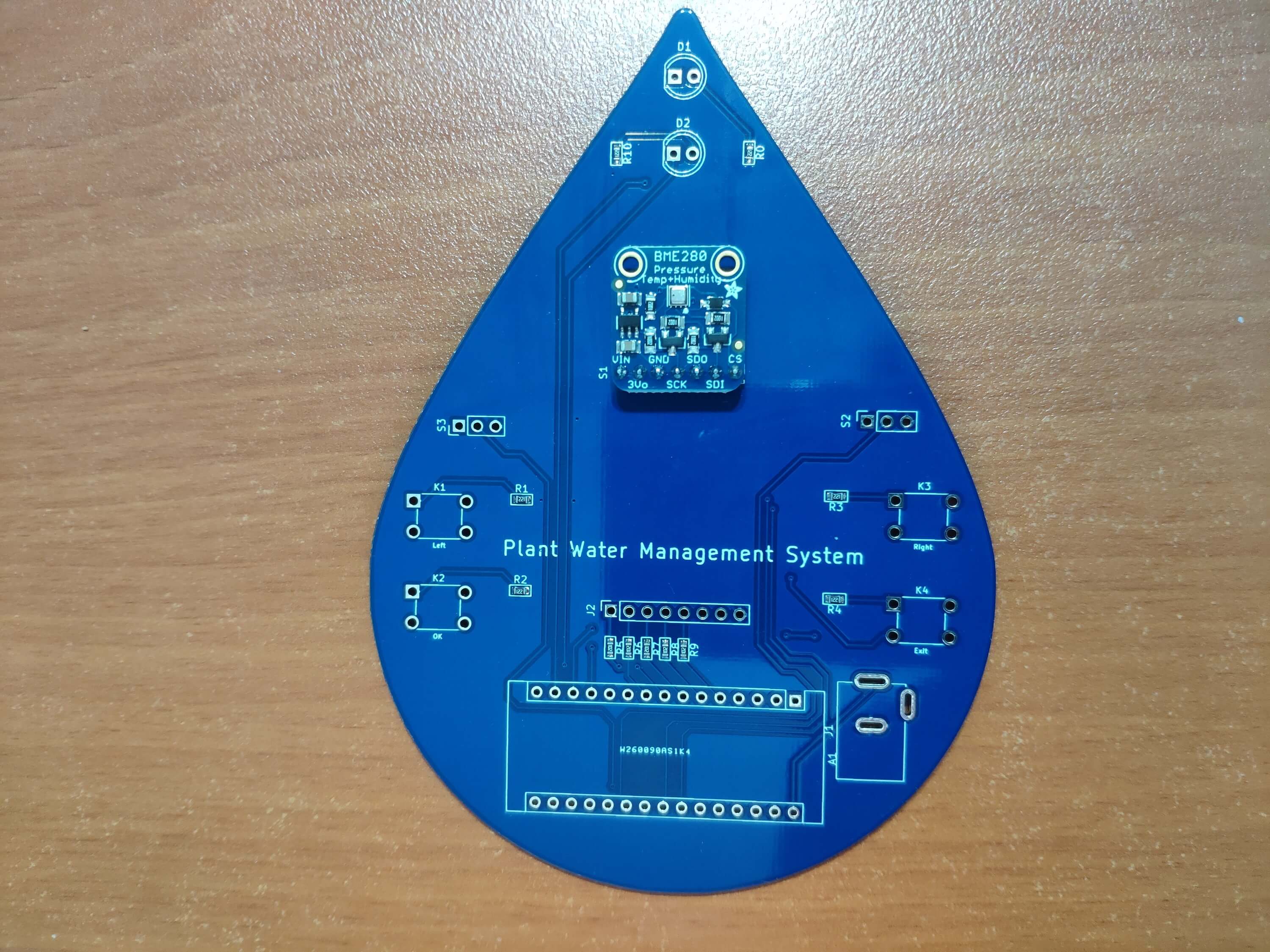
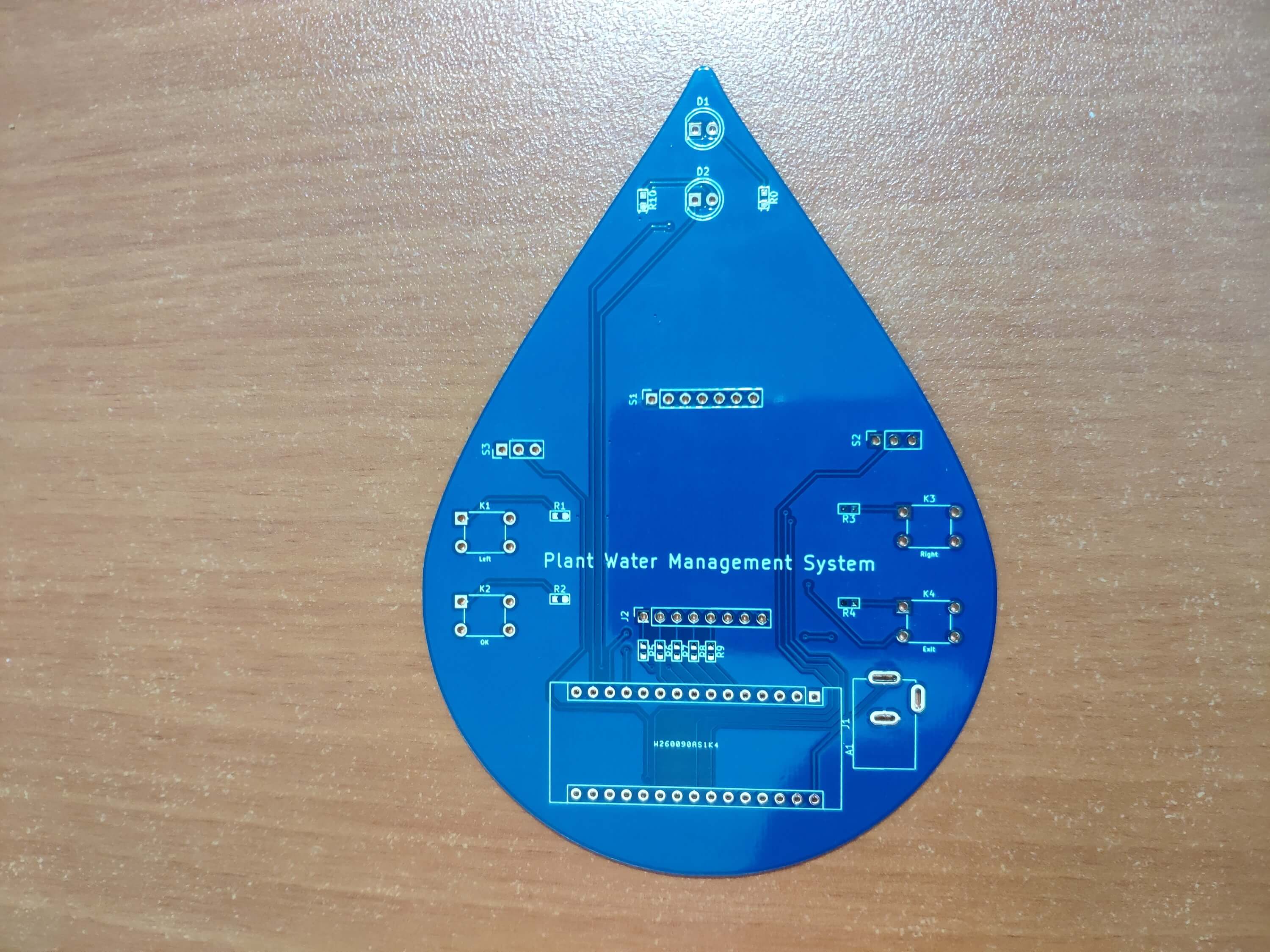
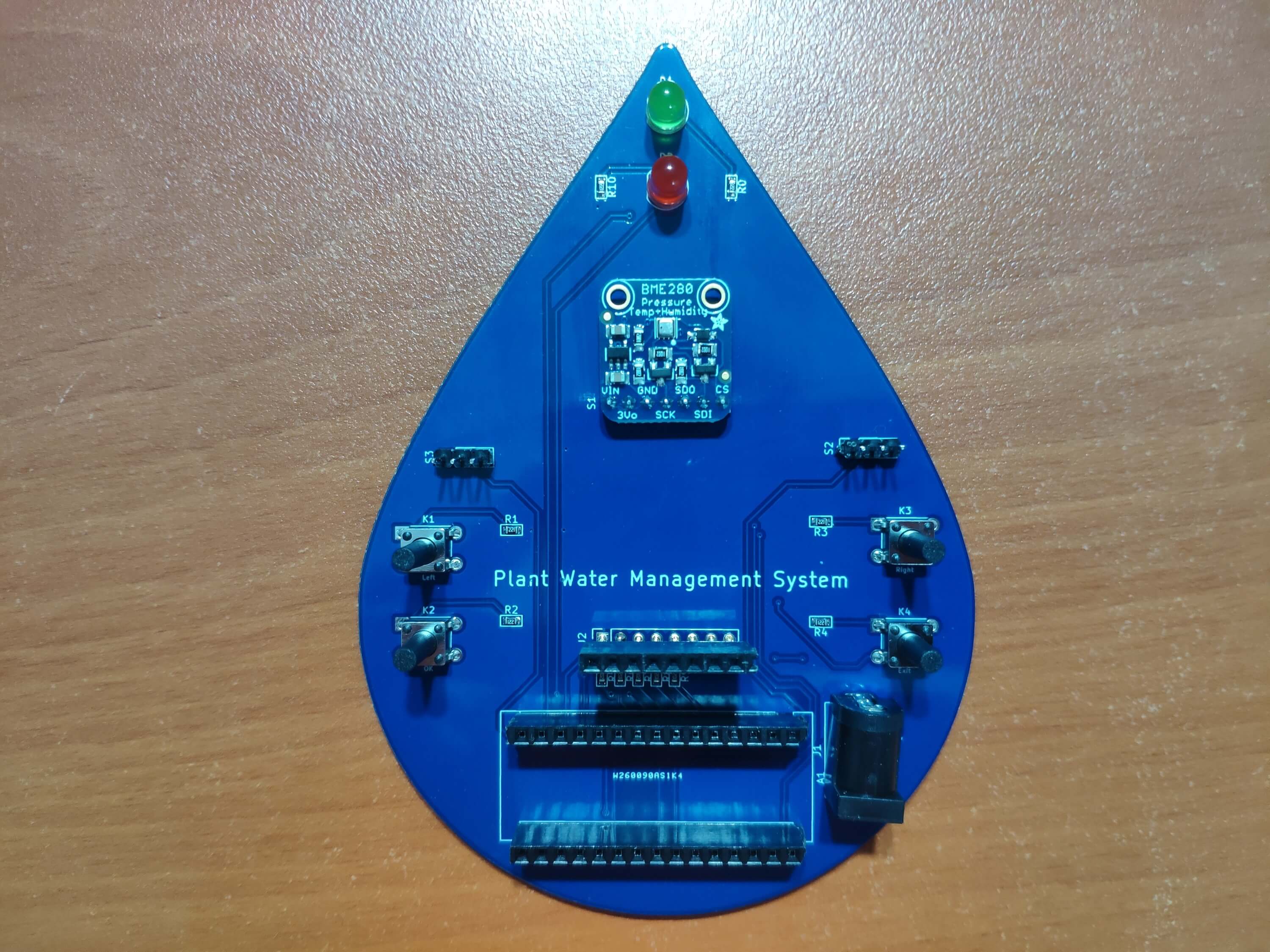
As a starting point for you, I will explain how I create a custom shape (water drop) PCB for one of my projects by using images in KiCad step-by-step. After I designed the PCB, I manufactured the custom design with PCBWay: their service is fast, reliable, and cheaper than most of the other brands in the market for custom shape PCBs. As intended, after manufacturing, I received a unique water-drop shaped PCB design for my project.
Step 1: Creating a new project in KiCad
- Open KiCad and click File -> New -> Project.
- Enter the name of your project - water_drop - and click Save.
Figure - 137.1
Step 2: Choosing an image for creating a custom board shape (Edge Cuts) in the right format
- According to your project design, choose a black and white picture - logo or icon - not including overlapping or contradicting lines. Otherwise, KiCad cannot detect lines and points properly to create Edge Cuts and throw an error message when reviewing the board.
Figure - 137.2
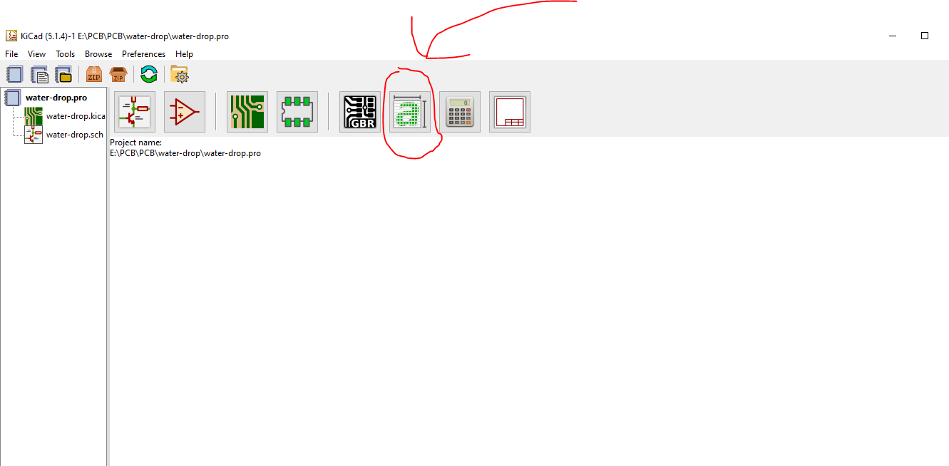
Step 3: Converting the image to the Edge Cuts
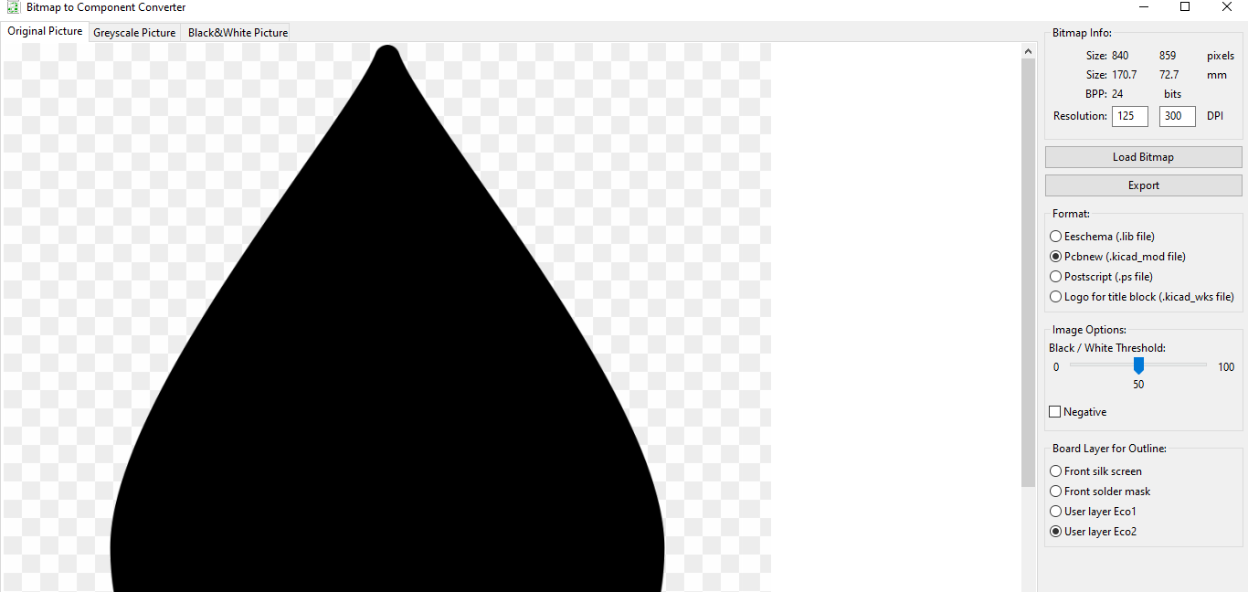
- Open the Bitmap to Component Converter and click Load Bitmap to upload the image - drop.png.
Figure - 137.3
- Adjust the size of the board by changing variables in the Resolution.
Figure - 137.4
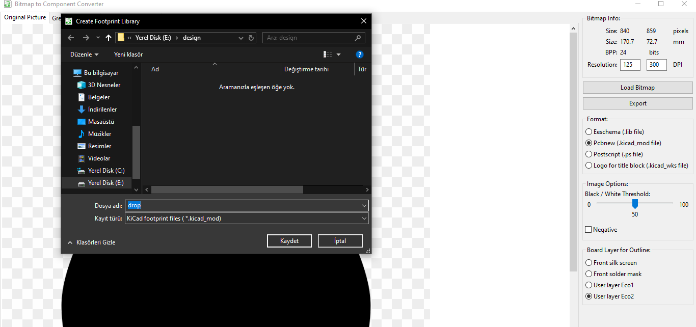
- Then, click Export and save the file as drop.kicad_mod.
Figure - 137.5
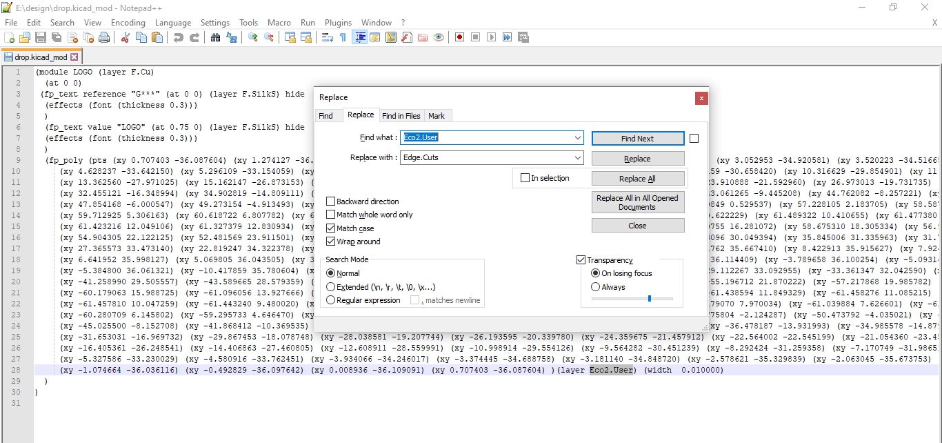
- Open the drop.kicad_mod file with a text editor and replace Eco2.User with Edge.Cuts.
Note: Module (LOGO), reference (G***), and value (LOGO) variables are also changeable.
Figure - 137.6
- Now, create a folder named drop.pretty and move the drop.kicad_mod file into that folder.
Figure - 137.7
Step 4: Adding the footprint (drop.pretty) to the project
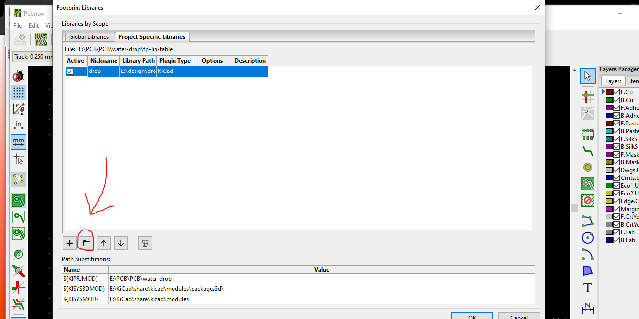
- Click Project Specific Libraries -> Add existing libraries to table to add the drop.pretty folder. Then, click OK.
Figure - 137.10
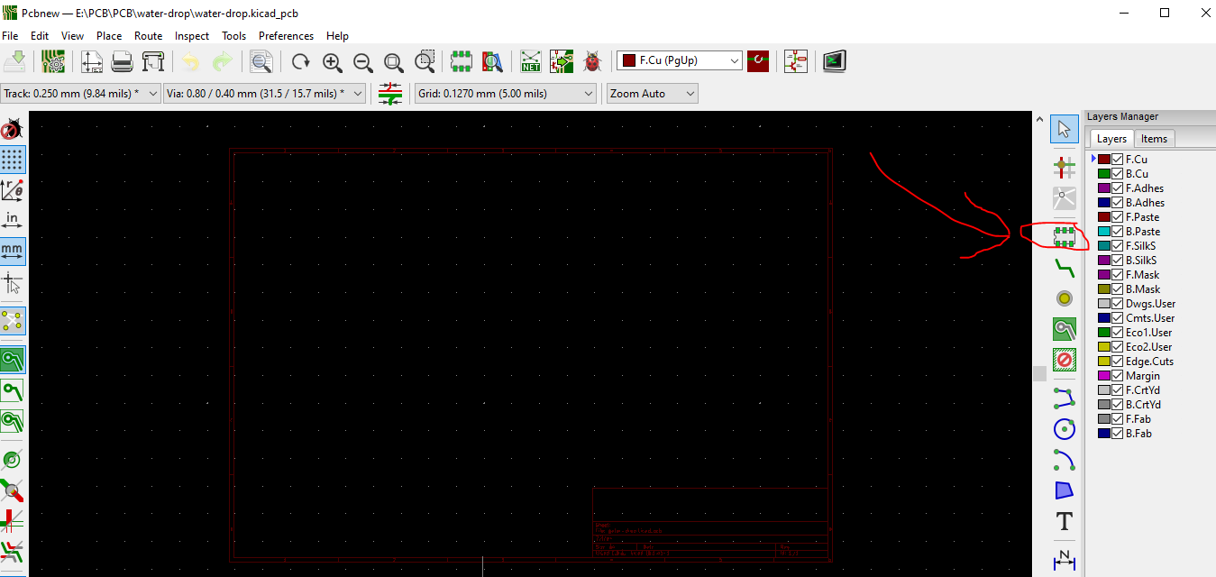
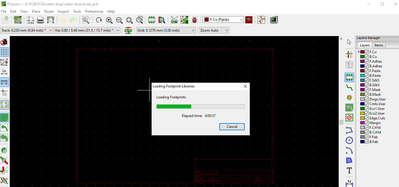
- Click Add footprints and wait until loading all libraries.
Figure - 137.11
Figure - 137.12
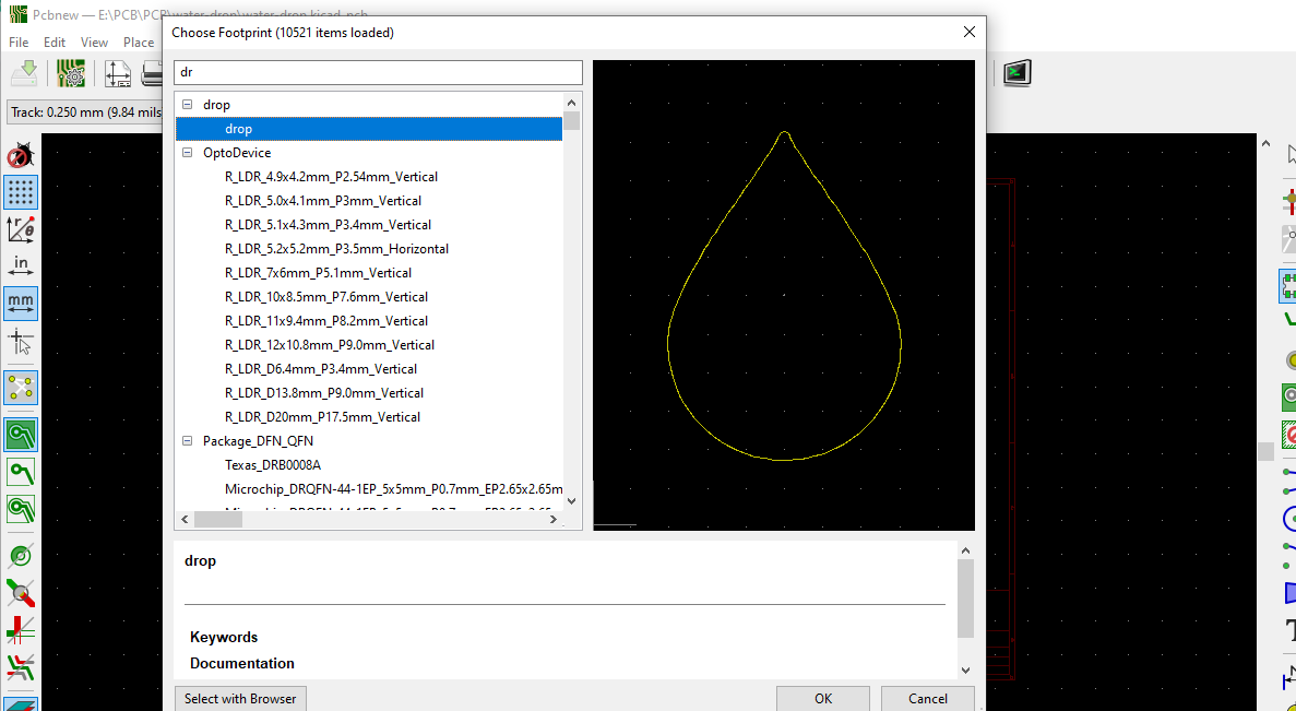
- Select drop and click OK to include the Edge.Cuts track to the project.
Figure - 137.13
Figure - 137.14
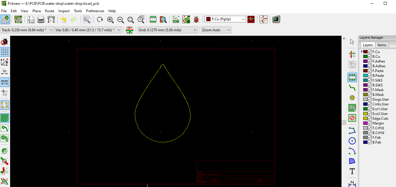
- Open the 3D Viewer to inspect the board.
Figure - 137.15
Step 5: Manufacturing the custom shape PCB with PCBWay
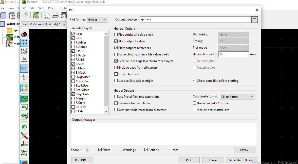
- After completing PCB component placing and connections, generate the Gerber files.
Figure - 137.16
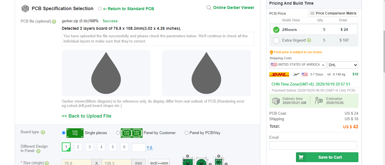
- Then, open the PCB Instant Quote on PCBWay and add the Gerber files.
- After setting PCB specifications depending on your project's features, the board is ready to be fabricated.
Figure - 137.17
Conclusion
I designed a custom shape PCB by following the same method for one of my projects and then manufactured the board with PCBWay, as explained above. Also, as did I, if you need PCBA with fast delivery time and accuracy, you can try PCBWay's PCB Assembly service.
Click here to inspect my project in which I utilized the custom shape PCB below.